- 您现在的位置:买卖IC网 > Sheet目录1992 > CY28378OXC (Silicon Laboratories Inc)IC CLOCK CK408/TITAN 845 48SSOP
CY28378
........................ Document #: 38-07519 Rev. ** Page 7 of 21
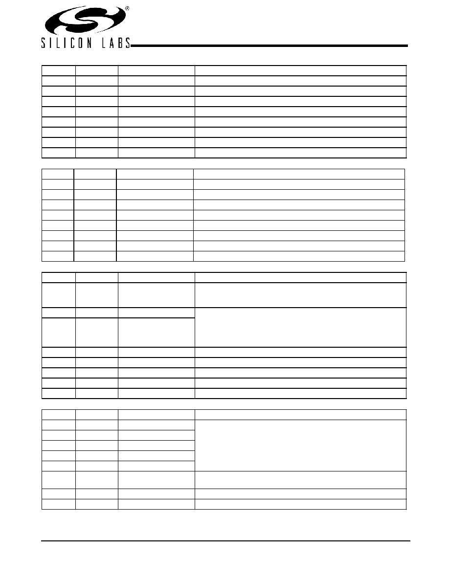
Byte 2
Bit
@pup
Name
Pin Description
Bit 7
0
Reserved
Bit 6
1
PCI6
(Active/Inactive)
Bit 5
1
PCI5
(Active/Inactive)
Bit 4
1
PCI4
(Active/Inactive)
Bit 3
1
PCI3
(Active/Inactive)
Bit 2
1
PCI2
(Active/Inactive)
Bit 1
1
PCI1
(Active/Inactive)
Bit 0
1
PCI0
(Active/Inactive)
Byte 3
Bit
@Pup
Name
Pin Description
Bit 7
1
PCI_F2
(Active/Inactive)
Bit 6
1
PCI_F1
(Active/Inactive)
Bit 5
1
PCI_F0
(Active/Inactive)
Bit 4
0
Reserved
Bit 3
1
CPU_ITP, CPU_ITP#
(Active/Inactive)
Bit 2
0
Reserved
Bit 1
1
REF1
(Active/Inactive)
Bit 0
1
REF0
(Active/Inactive)
Byte 4
Bit
@Pup
Name
Pin Description
Bit 7
0
MULTSEL_Override
This bit control the selection of IREF multiple.
0 = HW control; IREF multiplier is determined by MULTSEL[0:1] input pins
1 = SW control; IREF multiplier is determined by Byte[4], Bit[5:6].
Bit 6
HW
SW_MULTSEL1
IREF multiplier
00 = Ioh is 4 x IREF
01 = Ioh is 5 x IREF
10 = Ioh is 6 x IREF
11 = Ioh is 7 x IREF
Bit 5
HW
SW_MULTSEL0
Bit 4
0
Reserved
Bit 3
0
Reserved
Bit 2
0
Reserved
Bit 1
0
Reserved
Bit 0
0
Reserved
Vendor Test Mode (always program to 0)
Byte 5
Bit
@Pup
Name
Pin Description
Bit 7
HW
Latched FS4 input
Latched FS[4:0] inputs. These bits are read only.
Bit 6
HW
Latched FS3 input
Bit 5
HW
Latched FS2 input
Bit 4
HW
Latched FS1 input
Bit 3
HW
Latched FS0 input
Bit 2
0
FS_Override
0 = Select operating frequency by FS[4:0] input pins
1 = Select operating frequency by SEL[4:0] settings
Bit 1
0
SEL 3V66
0 = 48-MHz output on pin 27, 1 = 66-MHz output on pin 27
Bit 0
1
SEL 48MHZ
0 = 24-MHz,1 = 48-MHz
发布紧急采购,3分钟左右您将得到回复。
相关PDF资料
CY284108ZXC
IC CLOCK SERV CK410B 56TSSOP
CY28410OXC-2
IC CLOCK CK410 GRANTSDALE 56SSOP
CY28410OXC
IC CLOCK CK410 GRANTSDALE 56SSOP
CY28411ZXC
IC CLOCK CK410M ALVISO 56TSSOP
CY28442ZXC-2
IC CLOCK ALVISO PENTM 56TSSOP
CY28445LFXC-5
IC CLOCK CALISTOGA CK410M 68QFN
CY28446LFXC
IC CLOCK CALISTOGA CK410M 64QFN
CY28447LFXC
IC CLOCK CALISTOGA CK410M 72QFN
相关代理商/技术参数
CY28378OXCT
功能描述:时钟发生器及支持产品 Sys Clk Pentium 4 & Intel Brookdale 845 RoHS:否 制造商:Silicon Labs 类型:Clock Generators 最大输入频率:14.318 MHz 最大输出频率:166 MHz 输出端数量:16 占空比 - 最大:55 % 工作电源电压:3.3 V 工作电源电流:1 mA 最大工作温度:+ 85 C 安装风格:SMD/SMT 封装 / 箱体:QFN-56
CY28381
制造商:CYPRESS 制造商全称:Cypress Semiconductor 功能描述:High-Performance SiS645DX/648DX/650/651 Intel Pentium 4 Clock Synthesizer
CY28381OC
制造商:Rochester Electronics LLC 功能描述:- Bulk 制造商:Cypress Semiconductor 功能描述:
CY28381OCT
制造商:CYPRESS 制造商全称:Cypress Semiconductor 功能描述:High-Performance SiS645DX/648DX/650/651 Intel Pentium 4 Clock Synthesizer
CY28400
制造商:CYPRESS 制造商全称:Cypress Semiconductor 功能描述:100-MHz Differential Buffer for PCI Express and SATA
CY28400_05
制造商:CYPRESS 制造商全称:Cypress Semiconductor 功能描述:100-MHz Differential Buffer for PCI Express and SATA
CY28400-2
制造商:CYPRESS 制造商全称:Cypress Semiconductor 功能描述:100-MHz Differential Buffer for PCI Express and SATA
CY28400OC
功能描述:时钟缓冲器 100 MHz Diff Buffer PCI Express & SATA RoHS:否 制造商:Texas Instruments 输出端数量:5 最大输入频率:40 MHz 传播延迟(最大值): 电源电压-最大:3.45 V 电源电压-最小:2.375 V 最大功率耗散: 最大工作温度:+ 85 C 最小工作温度:- 40 C 封装 / 箱体:LLP-24 封装:Reel